|
New Portable Signal Generator
GED completed development of a portable RF Signal Generator Ranging from 1 to 2 GHz with 100kHz Resolution. The generator is fully
PC-programmable and features programmable pre-set frequencies, amplitude control, disable outputs, automatic reference detect and many other features making it extremely versatile.
This is the newest member of our diverse family of frequency sythesizers.
|
|
Dielectric Resonator Oscillators (DRO) are used widely in today's electronic warfare, missile, radar and
communication systems. They find use both in military and commercial applications. The DROs are characterized
by low phase noise, compact size, frequency stability with temperature, ease of integration with other hybrid
MIC circuitries, simple construction and the ability to withstand harsh environments.
These characteristics make DROs a natural choice both for fundamental oscillators and as the sources for
oscillators that are phase-locked to reference frequencies, such as crystal oscillators.
This paper summarizes design techniques for DROs and the voltage- tuning DRO (VT-DRO), and presents measured
data for them including phase noise, frequency stability and pulsing characteristics.
Design Techniques
The design technique we will discuss is for a dielectric resonator (DR) to be used as a series feedback
element. Practically, a GaAs FET or a Si-bipolar transistor is chosen as the active device for the
oscillator portion of the DRO circuit. The Si-bipolar transistor is generally selected for lower phase
noise characteristics, while the GaAs FET is required for higher frequencies.
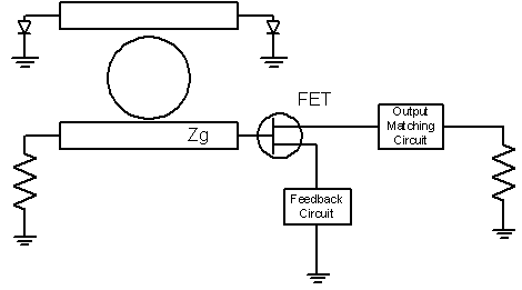
For example, a DRO with a DR as a series feedback element can be designed using following design procedure:
- Select an active device that is capable of oscillation at the design frequency, and use the small
signal S-parameter of the device for the design.
- Add a feedback circuit to ensure that the stability factor of the active device with the feedback
circuit is less than unity with enough margin.
- Create an active one-port analysis that consists of the active device, the feedback circuit, the
matching network and the load as shown as figure1. Optimize Za (?) with the parameters in the feedback
circuit and in the matching network to ensure that Ra (?0) is less than or equal to -25 ohms and Xa (?)
has the possible maximum variation near resonance in order to insure high circuit Q.
| Figure 1. Schematic diagram of the series feedback DRO. |
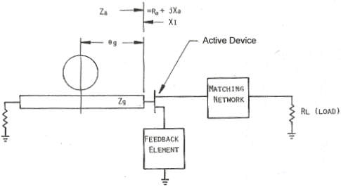 |
Determine the electrical spacing of the dielectric resonator such that the reactance it presents to the base
or gate of the transistor is the negative of Za. The characteristic impedance of the output transmission line,
Zg, is usually selected to be 50 ohms.
The open stub (characteristic impedance of 50 ohms), which is terminated at the source end of the FET, serves
as the feedback element. By adjusting the electric length of the feedback stub, various port impedance
characteristics for Za (?) in the band of interest (6-15 GHz) can be obtained.
From the port reactance characteristic, we observe that the shorter the electric length of feedback stub, the
more rapid the port reactance change with frequency. On the other hand, for the active port, a shorter
feedback stub induces higher negative resistance.
Finally, negative resistance is reduced if the electrical length of the feedback stub is less than 25 degrees.
Taking etch tolerances into consideration, the length of the feedback stub is chosen as 45 degrees.
10 GHz Example:
The resultant input impedance of the active port is Za = -40.8 -j62.5 ohms at the desired frequency. The
negative resistance of -40.8 ohms is sufficient to allow the transistor to build up and sustain oscillation at
the desired frequency.
It remains to determine the length of a 50 ohm terminated microstrip line between the coupling plane of the DR
and the gate terminal of the active device. We know that the load must have a reactance XI = 62.5 ohms to
resonate with the reactance of the active device input (gate) port.
Looking toward the DR from this port, the circuit appears as if it were an open circuited transmission line
stub for which the open circuit appears at the equivalent coupling plane of the DR, about equal to the
location of the DR's centerline drawn perpendicular to the line to which it couples. Accordingly, its
reactance is XI = Zg cot (?g), from which the spacing of the DR can be determined. In the present series
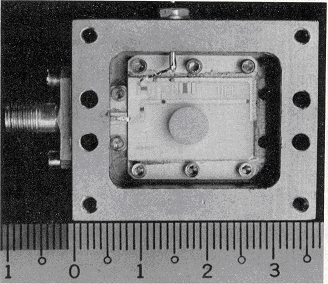
feedback example, the computed electric length is 141.3 degrees at 10.4 GHz. A photograph of the 10.4 GHz DRO
is shown in
| Figure 2. Photograph of a 10GHz DRO. |
 |
Small signal S parameters are used in the design, whereas in reality the oscillator's voltage amplitudes
increase until saturation, at which the DRO reaches its steady state output power. This saturation, by
definition, corresponds to the high level S parameter case. Nevertheless, designs based upon the small signal
behavior are found to yield a good first order solution, requiring minor adjustment for high level operation
at the desired frequency.
The frequency stability of the DRO over temperature is selected by taking into account the total circuit. In
other words, the temperature characteristics of the supporting structure, the epoxy with which the DR is
attached, the RF device, and the circuit housing must be accounted for during selection of the dielectric
resonator material and temperature coefficient.
A frequency stability of 3 parts per million per degree Centigrade (3 ppm/C°) for a DRO operating around 10
GHz is typically achievable. This corresponds to a frequency shift of 30 kHz per Centigrade degree shift.
Differences in DR Material
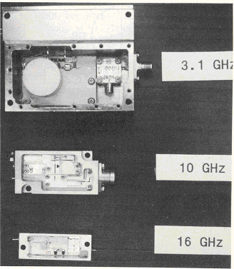
Besides temperature coefficient, the DR is selected for its size and dielectric constant. Figure 3 shows that
the size of the DR (the thickness to diameter ratio of a DR is generally kept to 0.4 for the widest mode
separation) is inversely proportional to the frequency of the DRO for the same dielectric material.
| Figure 3. Picture of DRO of different diameters for close to the same freq. |
 |
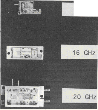
On the other hand, Figure 4 shows that dielectric resonators of almost the same size but with different
dielectric materials can be used for DROs of various frequencies. The 12 GHz DRO with integral amplifier shown
has the smallest size (0.515" x 0.535" x 0.375") ever reported using hybrid MIC techniques, yet it delivers
more than 20 dBm of output power at 105 C°.
| Figure 4. DROs of different frequencies with different dielectric material used for the CRs |
 |
Electronic Frequency Tuning
Frequency tuning of a DRO can be achieved by using voltage controlled diodes (varactors). The circuit
configuration for coupling the varactors to the DR consists of an additional line paralleling that which
couples the DR to the active device, and placed on the opposite side of the DR see figure 5. In the example
shown two varactors are attached to the ends of a microstrip half wavelength resonator having characteristic
impedance Zt.
| Figure 5a. Schematic of VT-DRO. |
 |
At the DR plane of coupling, the transmission line can be treated as two quarter-wavelength impedance
transformers (or, more precisely two impedance inverters) terminated with two tuning varactors. The
varactors' capacitive variation at the end of the inverter is transformed into inductive variation at the
plane of the coupling by the impedance inverter.
By increasing the coupling between the DR and the varactor/microstrip line, the tuning bandwidth of the DRO
can also be increased. There is a trade-off for wider tuning bandwidth in that degraded phase noise and poorer
frequency stability results, mainly due to the resultant equivalent degradation in the unloaded Q of the
dielectric resonator.
Keeping this in mind, it is necessary that the electrical tuning band of the DRO be wider than the anticipated
frequency drift of the oscillator versus temperature.
In summary, coupling the dielectric resonator to the tuning line and coupling the tuning circuit to the
oscillator circuit must be kept in balance. Than can easily be done without significantly degrading the phase
noise characteristics or temperature performance.
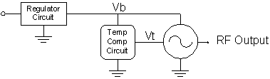
Temperature Compensation DROs
Electrical tuning of a DRO can be used to compensate for frequency drift over temperature. The DRO frequency
change over temperature is measured for various temperatures to establish a frequency drift profile. A
correction profile is calculated and a correction circuit consisting of thermistors (resistors that very with
temperature) and resistors is calculated. This temperature sensor information is converted into proper tuning
voltage and is fed into the tuning port of the DRO.
| Figure 5b. Block diagram of Temperature Compensated DRO (TC-DRO). |
 |
This compensation technique is well known in TCXOs and the three or four typical compensation profiles are
well established and easily fabricated.
The temperature compensated DROs using the analog approach exhibit + /- 0.3 ppm per degree C stability with
DRO output frequencies up to 20 GHz from and over the temperature range -54 C to + 105 degrees C.
| Figure 6. TC-DRO temperature profile. |
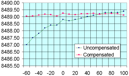 |
The analog approach is smooth and continuous with no thermal toggling. The digital approach of temperature
compensation also can provide similar frequency stability but much more complex circuitry is required.
Phase Locked Loop DROs
The VT-DRO can be used in conjunction with a sampling phase detector (SPD) to form the correction loop of a
phase-locked source. The main advantage of PLL-DRO is its superior phase noise performance. Inside the loop,
the phase noise has the characteristics of a frequency up-converted crystal oscillator [20log(N)] and outside
the loop, the phase noise is the VT-DRO. The loop bandwidth can be shifted in frequency to minimize the loop
circuit noise peaking.
| Figure 7. Noise plot of PLL-DRO |
 |
The tuning sensitivity ratio (frequency change versus control voltage) is relatively consistently, which makes
the loop circuit relatively consistent. The low phase noise and small circuit size make the VT DRO very
attractive in phase-locked source applications.
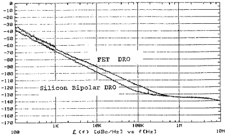
Phase Noise
One of the important characteristics of a DRO is its phase noise at 10 kHz or higher away from the carrier.
The phase noise of a DRO is dependent upon the active device used, the coupling of oscillation power to the
DR, and the amount of power delivered to load. Figure 10 shows the typical phase noise characteristics of a
DRO using Si-bipolar transistors and GaAs FETs. The Si-bipolar transistor provides about a 10 dB improvement
in phase noise, which is generally believed to be contributed by Vfm noise of the GaAs FETs. Phase noise
increases with the square of operating frequency, thus to obtain the phase noise level of a DRO at frequencies
other than 10 GHz, add 20x log10 [f(GHz)/10] to the values shown in Figure 10. For example, corresponding
phase noise will be 6 dB greater for a 20 GHz DRO.
As more energy is stored in the dielectric resonator, the temperature characteristic of the DRO more closely
follows that of the DR, however more of the active device's power is dissipated in the DR, leaving less for
output. Also the phase noise of the DRO also may degrade. Therefore, some compromise often must be made
between the DRO's temperature stability and phase noise.
Pulsing Characteristics
For some applications it is desirable that the output power of the DRO be turned on and off, subjected to
pulsing from TTL control signals. Pulsing circuitries can be placed at the drain (Figure 12a) or at the
ground (Figure 12b). Both circuits yield similar pulsing rise time, defined as the time between 50% TTL
input and 90% RF output. A rise time 600 nsec has been obtained for a 16 GHz DRO with 20 dBm output power
and phase noise of 86 dBc/Hz at 10 kHz from the carrier. The high unloaded Q (Qu) nature of the DR
requires longer time to build up the energy in the resonator compared a free running oscillator.
To increase the pulsing speed, relatively high loss dielectric resonator material can be used together
with tighter coupling of the microstrip line to the DR, at the expense of reduced unloaded Q and
significant impact on phase noise and frequency stability. While the frequency stability of a DRO can be
compensated by using a DR of proper temperature characteristics, the phase noise appears to be the
parameter that must be traded off for faster rise time pulsing. A similar design of a DRO at 16 GHz, when
optimized for pulse rise time, exhibits less than 100 nsec rise time but a phase noise degraded to 73
dBc/Hz at 10 kHz from the carrier.
The settling time of the fast pulsing DRO is less than 100 nsec when the frequency is measured with 80 +1/
-100 kHz referenced to the frequency measured at 500 nsec and drift within +1/ -100 kHz from 500 nsec to 1
sec.
References
- Kajfez, D. and Guillon, P., Dielectric Resonators, Artech House, 1986, Chapter 10.
- Soares, R., GaAs MESFET Circuit Design, Artech House, 1988, Chapter 7.
- Anderson, K. and Pavio, A., "FET Oscillators Still Require Modelling, But Computer Techniques Simplify the Task", MSN, September 1983, pp. 62-73.
- Chen, S. et ai, "A Unified Design of Dielectric Resonator Oscillator for Telecommunication Systems," IEEE-MTTS Digest, 1986, pp. 593-596.
- Lee, K. and Day, W., "Varactor-Tuned Dielectric Resonator GaAs FET Oscillator in X-Band," IEEE-MTTS Digest, 1982, pp. 274-276.
- Liu, C and Ho, C, "On the Design of a Voltage-Tuned Push-Push DRO", to appear in April 1990 issue of Microwave Journal.
- Pavio, A. and Smith, M., "Push-Push DRO," IEEE-MTTS Digest, 1985, pp. 268-269.
- "DRO Catalog," MIA-COM, 1987.9. "Dielectric Resonator Oscillator," Applications Note by Varian.
|
|
320 South Pacific St.
San Marcos, CA 92078

|
| Phone: | (760) 591-4170
(760) 591-4095 |
|---|
| Fax: | (760) 591-4164 |
|---|
| Email: | info@gedlm.com |
|---|
|
